- 您现在的位置:买卖IC网 > Sheet目录1905 > ATMEGA328P-15AZ (Atmel)MCU AVR 32K FLASH 15MHZ 32-TQFP
2010-2012 Microchip Technology Inc.
DS41413C-page 177
PIC12(L)F1822/PIC16(L)F1823
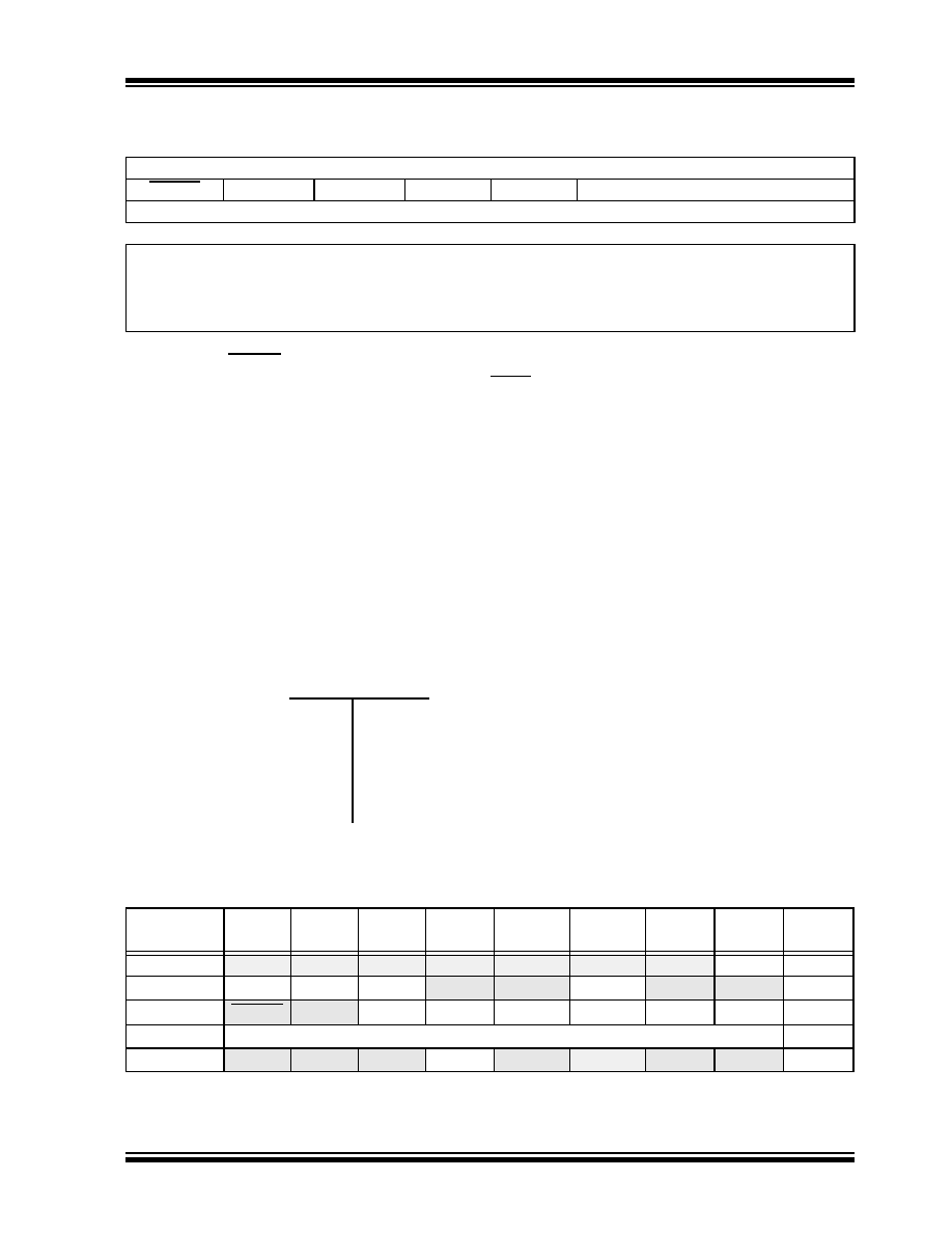
TABLE 20-1:
SUMMARY OF REGISTERS ASSOCIATED WITH TIMER0
REGISTER 20-1:
OPTION_REG: OPTION REGISTER
R/W-1/1
WPUEN
INTEDG
TMR0CS
TMR0SE
PSA
PS<2:0>
bit 7
bit 0
Legend:
R = Readable bit
W = Writable bit
U = Unimplemented bit, read as ‘0’
u = Bit is unchanged
x = Bit is unknown
-n/n = Value at POR and BOR/Value at all other Resets
‘1’ = Bit is set
‘0’ = Bit is cleared
bit 7
WPUEN:
Weak Pull-up Enable bit
1
= All weak pull-ups are disabled (except MCLR, if it is enabled)
0
= Weak pull-ups are enabled by individual WPUx latch values
bit 6
INTEDG:
Interrupt Edge Select bit
1
= Interrupt on rising edge of RB0/INT pin
0
= Interrupt on falling edge of RB0/INT pin
bit 5
TMR0CS:
Timer0 Clock Source Select bit
1
= Transition on RA4/T0CKI pin
0
= Internal instruction cycle clock (FOSC/4)
bit 4
TMR0SE:
Timer0 Source Edge Select bit
1
= Increment on high-to-low transition on T0CKI pin
0
= Increment on low-to-high transition on T0CKI pin
bit 3
PSA:
Prescaler Assignment bit
1
= Prescaler is not assigned to the Timer0 module
0
= Prescaler is assigned to the Timer0 module
bit 2-0
PS<2:0>:
Prescaler Rate Select bits
000
001
010
011
100
101
110
111
1 : 2
1 : 4
1 : 8
1 : 16
1 : 32
1 : 64
1 : 128
1 : 256
Bit Value
Timer0 Rate
Name
Bit 7
Bit 6
Bit 5
Bit 4
Bit 3
Bit 2
Bit 1
Bit 0
Register
on Page
CPSCON0
CPSON
CPSRM
—
CPSRNG1 CPSRNG0 CPSOUT
T0XCS
INTCON
GIE
PEIE
TMR0IE
INTE
IOCIE
TMR0IF
INTF
IOCIF
OPTION_REG WPUEN INTEDG TMR0CS TMR0SE
PSA
PS2
PS1
PS0
TMR0
Timer0 Module Register
TRISA
—
TRISA5
TRISA4
TRISA3
TRISA2
TRISA1
TRISA0
Legend:
— = Unimplemented locations, read as ‘0’. Shaded cells are not used by the Timer0 module.
* Page provides register information.
发布紧急采购,3分钟左右您将得到回复。
相关PDF资料
ATMEGA32L-8PJ
IC MCU AVR 32K 5V 8MHZ 40-DIP
ATMEGA32M1-AUR
IC MPU AVR 32K 20MHZ 32TQFP
ATMEGA48PA-MMNR
MCU AVR 4KB FLASH 20MHZ 28QFN
ATMEGA644P-B15MZ
IC MCU 8BIT 64KB FLASH 32VQFN
ATMEGA644V-10PU
IC AVR MCU FLASH 64K 40DIP
ATMEGA645V-8MI
IC AVR MCU FLASH 64K 1.8V 64QFN
ATMEGA649-16MI
IC AVR MCU FLASH 64K 5V 64QFN
ATMEGA649V-8MI
IC AVR MCU FLASH 64K 1.8V 64QFN
相关代理商/技术参数
ATMEGA328P-15MZ
功能描述:8位微控制器 -MCU 32KB In-system Flash 20MHz 1.8V-5.5V RoHS:否 制造商:Silicon Labs 核心:8051 处理器系列:C8051F39x 数据总线宽度:8 bit 最大时钟频率:50 MHz 程序存储器大小:16 KB 数据 RAM 大小:1 KB 片上 ADC:Yes 工作电源电压:1.8 V to 3.6 V 工作温度范围:- 40 C to + 105 C 封装 / 箱体:QFN-20 安装风格:SMD/SMT
ATMEGA328P-20AU
制造商:Atmel Corporation 功能描述:MCU 8-bit ATmega AVR RISC 32KB Flash 3.3V/5V 32-Pin TQFP
ATMEGA328P20MU
制造商:Atmel Corporation 功能描述:MCU 8-Bit ATmega AVR RISC 32KB Flash 3.3V/5V 32-Pin MLF
ATMEGA328P-AN
功能描述:8位微控制器 -MCU AVR 32K FLSH 2K SRAM 1KB EE-20 MHZ 105C RoHS:否 制造商:Silicon Labs 核心:8051 处理器系列:C8051F39x 数据总线宽度:8 bit 最大时钟频率:50 MHz 程序存储器大小:16 KB 数据 RAM 大小:1 KB 片上 ADC:Yes 工作电源电压:1.8 V to 3.6 V 工作温度范围:- 40 C to + 105 C 封装 / 箱体:QFN-20 安装风格:SMD/SMT
ATMEGA328P-ANR
功能描述:8位微控制器 -MCU AVR 32K FLSH 2K SRAM 1KB EE-20 MHZ 105C
RoHS:否 制造商:Silicon Labs 核心:8051 处理器系列:C8051F39x 数据总线宽度:8 bit 最大时钟频率:50 MHz 程序存储器大小:16 KB 数据 RAM 大小:1 KB 片上 ADC:Yes 工作电源电压:1.8 V to 3.6 V 工作温度范围:- 40 C to + 105 C 封装 / 箱体:QFN-20 安装风格:SMD/SMT
ATMEGA328P-AU
功能描述:8位微控制器 -MCU 32KB In-system Flash 20MHz 1.8V-5.5V
RoHS:否 制造商:Silicon Labs 核心:8051 处理器系列:C8051F39x 数据总线宽度:8 bit 最大时钟频率:50 MHz 程序存储器大小:16 KB 数据 RAM 大小:1 KB 片上 ADC:Yes 工作电源电压:1.8 V to 3.6 V 工作温度范围:- 40 C to + 105 C 封装 / 箱体:QFN-20 安装风格:SMD/SMT
ATMEGA328P-AU SL383
制造商:Atmel Corporation 功能描述:AVR 32K FLASH, 1K EE, 2K SRAM - 20 MHZ, TQFP, IND TEMP GREEN - Tape and Reel
ATMEGA328P-AUR
功能描述:8位微控制器 -MCU AVR 32K FLSH 2K SRAM 1KB EE-20MHz IND
RoHS:否 制造商:Silicon Labs 核心:8051 处理器系列:C8051F39x 数据总线宽度:8 bit 最大时钟频率:50 MHz 程序存储器大小:16 KB 数据 RAM 大小:1 KB 片上 ADC:Yes 工作电源电压:1.8 V to 3.6 V 工作温度范围:- 40 C to + 105 C 封装 / 箱体:QFN-20 安装风格:SMD/SMT